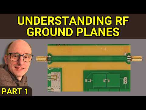
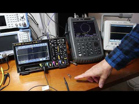
Free mini-course: Full course info: other videos - In this series, I'm going to show you some very simple rules to achieve the highest performance from your radio frequency PCB design for your electronics project. I'll do this by showing you how to improve the grounding and reduce the crosstalk. These rules apply to both analog , digital and RF electronics. I'll also share some rules of thumb for PCB parasitics that you can use in electronics simulations. I'll prove my points with actual measurements on dedicated test PCBs. In this third part, I'll focus on how to get the maximum from your 2 layer PCB design and the theory behind it. Website: 00:00 Introduction 00:30 Connecting top ground on a 4 layer PCB 02:21 Connecting top ground on a 2 layer PCB 05:07 Free design guide 05:32 2 layer vs 4 layer crosstalk 07:59 Crosstalk theory explained in detail 11:01 Crosstalk conclusions 12:07 The 2 layer solution 12:28 Plans for next test board and video
- 41350Просмотров
- 1 год назадОпубликованоHans Rosenberg
The Easiest Way to Fix Grounding Issues in 2-Layer PCBs
Похожее видео


Популярное
Новини